2026.06.16
Seminar
Research Group Homepage Launched

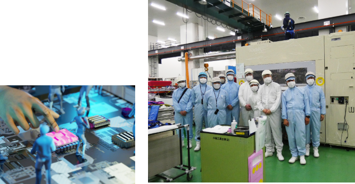
The SUMCO Joint Research Department of 3D-Si Integrated Device, led by Professor Kazunari Kurita, conducts advanced research on silicon wafer engineering for next‑generation CMOS image sensors. Our mission is to develop innovative device process technologies that enable the large‑scale manufacturing of 3D‑stacked backside‑illuminated CMOS image sensors for consumer electronics. To address critical challenges such as metallic impurity contamination, copper diffusion in TSV structures, and the limitations of intrinsic gettering (IG), our group explores molecular ion implantation, cluster‑enhanced bonding, and advanced annealing methods including microwave and ultra‑fast pulsed‑laser annealing.
Our research activities focus on establishing high‑gettering‑capability silicon wafer designs using multi‑element molecular ion implantation, developing ultra‑high‑dose implanted wafers with low‑thermal‑budget annealing, and investigating cluster‑enhanced surface activation for 3D wafer bonding. We also study Cu/Ru thin‑film surface chemistry in through-silicon-via (TSV) processes and develop high‑sensitivity analytical techniques such as Deep Level Transient Spectroscopy (DLTS), Electron Beam Induced Current (EBIC), and Time Domain Terahertz Spectroscopy (TDTS) for trace metallic impurity detection in advanced CMOS devices. These efforts contribute to solving fundamental reliability issues in modern imaging devices and support the evolution of 3D‑stacked semiconductor architectures.
This department operates as a collaborative initiative between Kyushu University and SUMCO Corporation, enabling the seamless integration of academic research with industrial expertise. Professor Kurita, a leading figure in gettering technology with over 200 patents and numerous invited presentations, brings more than three decades of combined academic and industrial experience. His contributions to proximity gettering, low‑temperature annealing, and impurity control have been widely recognized in journals such as IEEE JEDS, Sensors, and JJAP.
We actively welcome international students and postdoctoral researchers who wish to build their careers in semiconductor device engineering. Members of our group engage in hands‑on experimental research, publish in peer‑reviewed journals, and participate in international conferences. Our laboratory provides a globally connected environment where young researchers can grow through collaboration, innovation, and exposure to both academic and industrial perspectives. We invite motivated individuals from around the world to join us in advancing the future of solid‑state imaging devices.
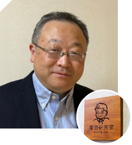
Professor
Kazunari Kurita
Center of Plasma Nano-Interface Engineering
SUMCO Joint Research Department
of 3D-Si Integrated Device
Kyushu University
Modern CMOS image sensors serve as ubiquitous components in consumer electronics, powering high-performance cameras in smartphones and tablets.
As market demand intensifies for enhanced sensitivity and high-speed data processing, the development of advanced structures such as 3D-stacked backside-illuminated CMOS image sensors have become imperative.

We aim to establish a silicon wafer design architecture optimized for ultimate gettering efficiency through the integration of multi-element molecular ion implantation. This technology targets the suppression of contamination effects and supports the fabrication of 3D-stacked backside-illuminated CMOS image sensors.

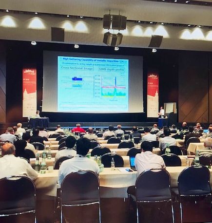
Members of the research group, led by Professor Kazunari Kurita, actively contribute to international, domestic conferences and academic workshops. The following list highlights key invited presentations that showcase research progress in gettering technology and advanced CMOS image sensor engineering.
We welcome inquiries and visits from prospective students and collaborators.
Please feel free to get in touch with us at the email address below:
Center for Plasma Nano-interface Engineering,
SUMCO Joint Research Department
of 3D-Si Integrated Device,
Kyushu University
744 Motooka Nishi-ku, Fukuoka 819-0395, Japan Room 653,
West-Building No.2
092-802-3737